 Article from Cnet:
In 1965, Intel co-founder Gordon Moore foresaw an inexorable rise in chip power that eventually delivered the computer to your pocket. While long in the tooth, Moore’s prediction still has plenty of life in it. Here’s why.
Year in, year out, Intel executive Mike Mayberry hears the same doomsday prediction: Moore’s Law is going to run out of steam. Sometimes he even hears it from his own co-workers.
But Moore’s Law, named after Intel co-founder Gordon Moore, who 47 years ago predicted a steady, two-year cadence of chip improvements, keeps defying the pessimists because a brigade of materials scientists like Mayberry continue to find ways of stretching today’s silicon transistor technology even as they dig into alternatives. (Such as, for instance, super-thin sheets of carbon graphene.)
Oh, and don’t forget the money that’s driving that hunt for improvement. IDC predicts chip sales will rise from $315 billion this year to $380 billion in 2016. For decades, that revenue has successfully drawn semiconductor research out of academia, through factories, and into chips that have powered everything from a 1960s mainframe to a 2012 iPhone 5.
The result: Moore’s Law has long passed being mere prognostication. It’s the marching order for a vast, well-funded industry with a record of overcoming naysayers’ doubts. Researchers keep finding ways to maintain a tradition that two generations ago would have been science fiction: That computers will continue to get smaller even as they get more powerful.
“If you’re only using the same technology, then in principle you run into limits. The truth is we’ve been modifying the technology every five or seven years for 40 years, and there’s no end in sight for being able to do that,” said Mayberry, vice president of Intel’s Technology and Manufacturing Group.
Plenty of other industries aren’t as fortunate. You don’t see commercial supersonic airplane travel, home fusion reactors, or 1,000-mile-per-gallon cars. But the computing industry has a fundamental flexibility that others lack: it’s about bits, not atoms.
“Automobiles and planes are dealing with the physical world,” such as the speed of sound and the size and mass of the humans they carry, said Sam Fuller, chief technology officer of Analog Devices, a chipmaker that’s been in the electronics business even longer than Intel. “Computing and information processing doesn’t have that limitation. There’s no fundamental size or weight to bits. You don’t necessarily have the same constraints you have in these other industries. There potentially is a way forward.”
That means that even if Moore’s Law hits a wall and chip components stop shrinking, there are other ways to boost computer performance.
Before we get too carried away with lauding Moore’s Law, be forewarned: Even industry optimists, Moore included, think that about a decade from now there could be trouble. Yes, all good things come to an end, and at some point those physical limits people have been predicting will turn out to be real.
To understand those limits and how they may be overcome, I talked to researchers at the big chip companies, academics, and industry gurus. I wanted to go beyond what what most of us think we know about semiconductors and hear it from the experts. Do they have doubts? What are they doing about those doubts? The overwhelming consensus among the chip cognescenti, I found, was, yes, there’s a stumbling block a decade or so from now. But don’t be surprised if we look back at that prediction 20 years from now and laugh.
Strictly speaking
Moore’s Law is named after Gordon Moore, who in a 1965 paper in Electronics Magazine observed an annual doubling in the number of chip elements called transistors. He refined his view in 1975 with a two-year cycle in an updated paper. “I didn’t think it would be especially accurate,” Moore said in 2005, but it has in fact proved to be. And now, Intel times its tick-tock clock to Moore’s Law, updating its chip architecture and its manufacturing technology on alternating years.
Here’s a very specific illustration of what Moore’s Law has meant. The first transistor, made in 1947 at Bell Labs, was assembled by hand. In 1964, there were about 30 transistors on a chip measuring about 4 square millimeters. Intel’s “Ivy Bridge” quad-core chips, the third-generation Core i7 found found in the newest Mac and Windows PCs, has 1.4 billion transistors on a surface area of 160 square millimeters — and there are chips with even more.
A transistor is the electrical switch at the heart of a microprocessor, similar to a wall switch that governs whether electric current will flow to light a lamp. A transistor element called a gate controls whether electrons can flow across the transistor from its “source” side to its “drain” side. Flowing electrons can be taken logically as a “1,” but if they don’t flow the transistor reads “0.” Millions of transistors connected together on a modern chip process information by influencing each other’s electrical state.
In today’s chips, a stretch of silicon connects the source to the drain. Silicon is a type of material known as a “semiconductor” because, depending on conditions, it’ll either act as a conductor that transmits electrons or as an insulator that blocks them. Applying a little electrical voltage to the transistor’s gate controls whether that electron current flows.
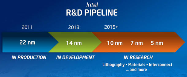
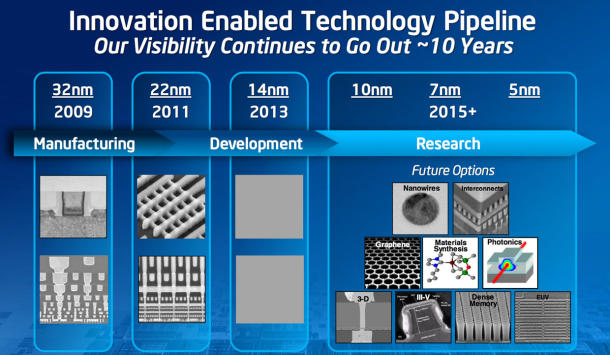
To keep up with Moore’s Law, engineers must keep shrinking the size of transistors. Intel, the leader in the race, currently uses a manufacturing process with 22-nanometer features. That’s 22 billionths of a meter, or roughly a 4,000th the width of a human hair. For contrast, Intel’s first chip, the 4004 from 1971, was built with a 10-micron (10,000-nanometer) process. That’s about a tenth the width of a human hair.
Intel’s Ivy Bridge generation of processors is an example of how hard it can be to sustain that process.
To make the leap from the earlier 32nm process to today’s 22nm process, Intel had to rework the basic “planar” transistor structure. Previously, the electrons traveled in a flat silicon channel laid flat into the plane of the silicon wafer and with the gate perched on top. To work around the limits of that approach, Intel flipped the planar transistor’s silicon on its side into a fin that juts up out of the plane of the chip. The gate straddles this fin the way a person might straddle a low fence with both legs. To improve performance, Intel can put as many as three of these fins in a single transistor.
The result is a “tri-gate” chip design that shrinks without suffering debilitating new levels of “leakage,” which takes place when current flows even when a transistor is switched off. And it means Intel has one more “shrink” of the chip manufacturing process under its belt.
Developing the tri-gate transistors wasn’t easy: Intel researchers built the company’s first finned transistor in 2002, nine years before it was ready for mass-market production. And it wasn’t the only challenge; other fixes include making gates out of metal, connecting transistors with copper rather than aluminum wires, and using “strained” rather than ordinary silicon for the channel between source and drain.
In 2013, Intel plans another shrink to a 14nm process. Then comes 10nm, 7nm, and, in 2019, 5nm.
And it’s not just Intel making up these numbers. In the chip business, a fleet of companies depend on coordinated effort to make sure Moore’s Law stays intact. Combining academic research results with internal development and cross-industry cooperation, they grapple with quantum-mechanics problems such as electron tunneling and current leakage — a bugaboo of incredibly tiny components in which a transistor sucks power even when it’s switched off.
Discussion
No comments yet.